In part 2 of this series I will show my progress on developing a DIY PCI Card using Alteras FLEX10K FPGAs.
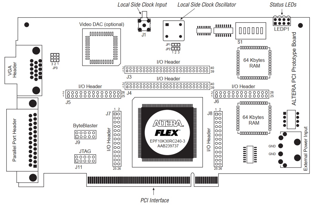
Last time I reverse-engineered an old Altera development-board I've found on eBay. Unfortunately there was absolutely no documentation about this card so I had to track all traces on the PCB by myself. Of course, I contacted some guys on Altera/Intel, but they couldn't help me as all old documents had been deleted. But they had another development-board for me - together with a helpful PDF-document: a FLEX 10K PCI Prototype Board with a single EPF10K30RC240-3 FPGA. The board has two 32kB SRAM-ICs, a VGA-Connector and lot of I/O-headers.
So I changed my Quartus 9 project to match the new device and the new pin-configuration. As written in my last post about this PCI-project, I already prepared the logic to read and write the configuration-space as well as basic IO-operation.
The first boot
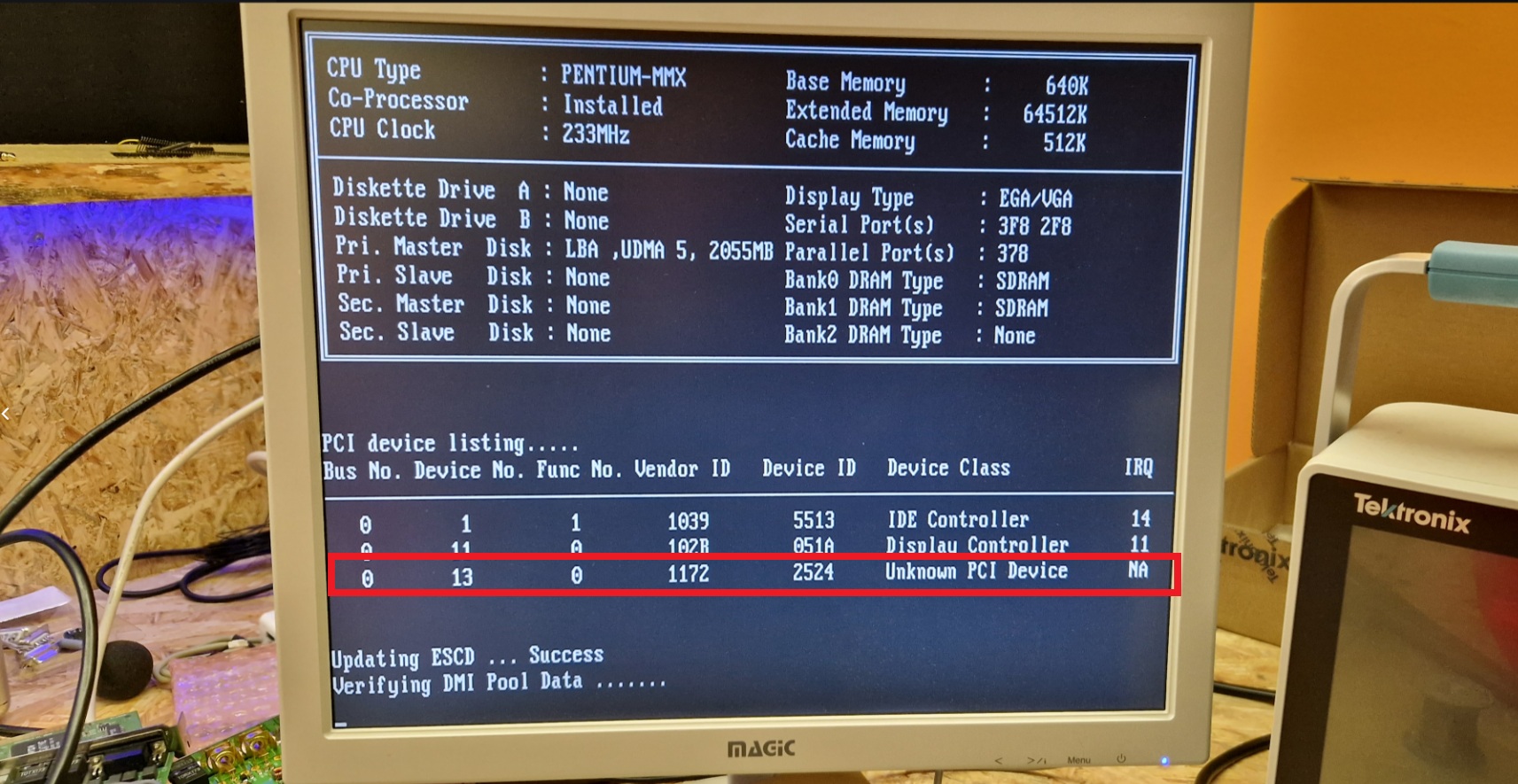
So I put the card into my Pentium 233 MMX testbench, turned on the computer, uploaded the logic to the card right after powering on and... the computer got stuck. Great. I removed lots of the logic, reuploaded the bitstream and... it started, but without recognizing my new card. Oh man. After a painful hour I realized, that I forgot to switch unused FPGA-pins to tristate by migrating the project to the new FPGA-type. Aaarrgh. So I reconfigured the unused output-pins, reuploaded the bitstream, reset the computer and: tadaaa, an "Unknown PCI Device" with my Vendor-ID 0x1172 and Device-ID 0x2524 showed up on the BIOS-screen:
Communication with the computer
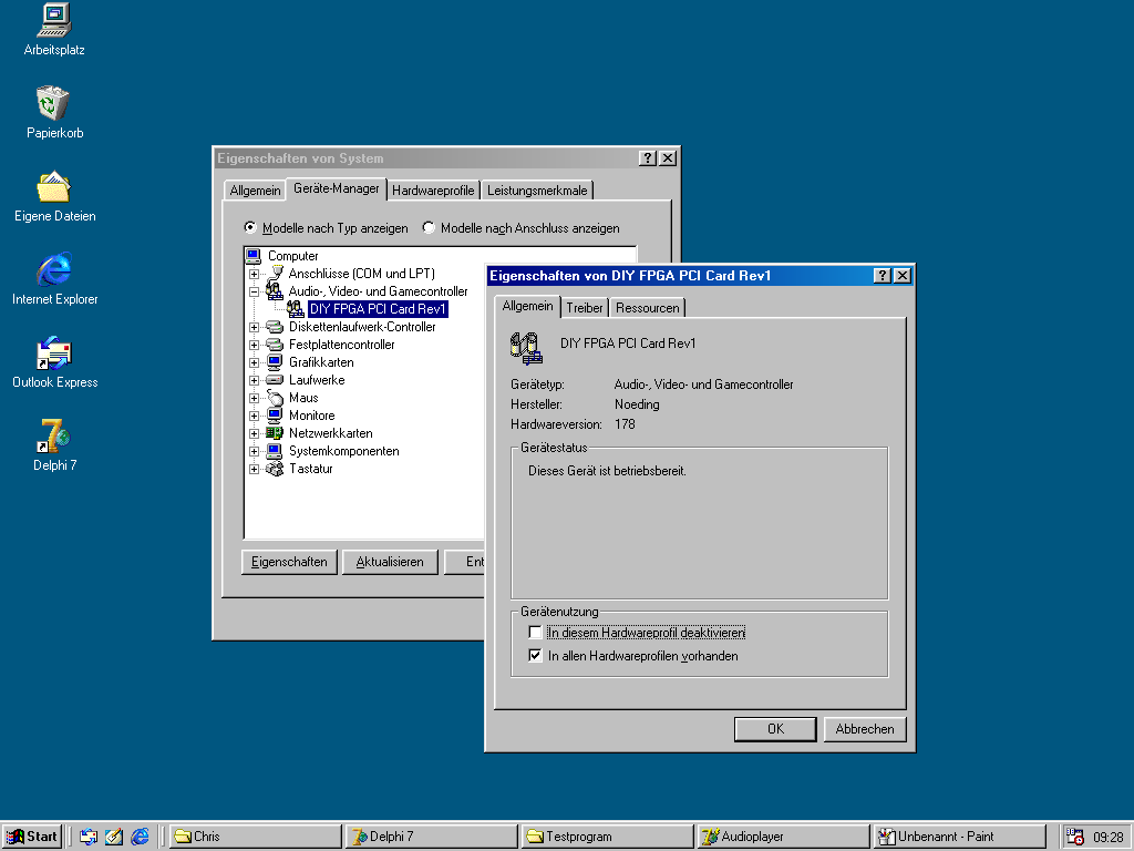
From now on the project took off. As my implementation of the configuration-space as well as the IO-space was working fine, the card was detected by the BIOS and the requested IO-range was assigned correctly. After setting the class-code to 0x048000 the card was detected as an "Multimedia Device". For now the memory-space is prepared, but not yet tested. To test the high-level functions of my card, I installed Windows 98SE on a CF-card and the device-manager showed up the device:
The configuration-space is defined using 16 DWORD-signals in VHDL:
conf_frame(0) <= x"25241172"; -- PID = 0x2524 | VID = 0x1172 = Altera
conf_frame(1) <= x"00000003";  -- status and command
conf_frame(2) <= x"048000B2";  -- ClassCode | revision ID = 0xB2
conf_frame(3) <= x"00000000"; -- Cache Line Size (CLS)
conf_frame(4) <= x"00000000"; -- BAR0 (we will register 16 bytes in IO-space)
conf_frame(5) <= x"00000000"; -- BAR1 (we will register 1MB bytes in memory-space)
conf_frame(6) <= x"00000000"; -- BAR2 (unused)
conf_frame(7) <= x"00000000"; -- BAR3 (unused)
conf_frame(8) <= x"00000000"; -- BAR4 (unused)
conf_frame(9) <= x"00000000"; -- BAR5 (unused)
conf_frame(10) <= x"00000000"; -- CardBus CIS Pointer
conf_frame(11) <= x"00001172"; -- SubSystemID (0x0000) | System Vendor ID (0x1172)
conf_frame(12) <= x"00000000"; -- Expansion ROM Base Address
conf_frame(13) <= x"00000000"; -- Reserved | Capabilities Pointer
conf_frame(14) <= x"00000000"; -- Reserved
conf_frame(15) <= x"00000200"; -- MaxLat | MinGnt | Interupt Pin | Interrupt Line
Lets have a look at the heart of the VHDL-code. After defining the above structure of the configuration-space, we have to wait until the PCI host requests data from this space. So we stay in an idle-state until the nFrame is asserted. If the read command equals "confread" (0b1010), then we take the DWORD-address and enter the confreadTurn-state on the next rising edge. When the nIRDY-signal is asserted we access the confread-state where the data is put to the 32 AD-lines. If the signals are placed, we assert the nTRDY to tell the host that we are ready. After another clock we jump back to the idle-state:
if (s_SM_Transaction = s_Idle) then
    -- stay in Idle until we received a start of bus cycle at nFrame

    -- disable all outputs
    AD_oe <= '0';
    PAR_oe <= '0';
    PAR_calc <= '0';
    nTRDY_io <= 'Z'; -- set outputs (bi-directional-pins) to High-Z
    nDEVSEL_io <= 'Z'; -- set outputs (bi-directional-pins) to High-Z
    nSTOP_io <= 'Z';
    rdy0_o <= '0';
    rdy1_o <= '0';
    rdy2_o <= '0';
    rdy3_o <= '0';

    if (nFrame_io = '0') then -- start of bus cycle is detected
        if (nCBE_io = confread and IDSEL_i = '1' and AD_io(1 downto 0) = "00") then
            -- take the DWORD-Address by ignoring the first two bits
            dataPointer <= to_integer(unsigned(AD_io(7 downto 2)));
            s_SM_Transaction <= s_confreadTurn;
        end if;

        -- ...
        -- here are more states like confwrite and ioread/iowrite
        -- ...
    end if;

elsif (s_SM_Transaction = s_confreadTurn) then
    -- wait one clock for the turnaround-cycle
    nDEVSEL_io <= '1';  -- deassert nDEVSEL
    nTRDY_io <= '1'; -- deassert nTRDY
    nSTOP_io <= '1';

    if (nIRDY_io = '0') then
        stateCounter <= 0;
        s_SM_Transaction <= s_confread;
    end if;

elsif (s_SM_Transaction = s_confread) then
    if (stateCounter = 0) then
        nDEVSEL_io <= '0';  -- assert nDEVSEL to tell master that we take this transaction
    elsif (stateCounter = 1) then
        nTRDY_io <= '0';    -- assert nTRDY to tell master that we are ready to send
    end if;

    AD_oe <= '1'; -- enable outputs
    nSTOP_io <= '1'; -- set outputs

    if (dataPointer <= 15) then
        -- output individual bytes using the byte-enabled-signal
        AD_o <= (conf_frame(dataPointer)(31 downto 24) and (7 downto 0 => (not nCBE_io(3)))) &
            (conf_frame(dataPointer)(23 downto 16) and (7 downto 0 => (not nCBE_io(2)))) &
            (conf_frame(dataPointer)(15 downto 8) and (7 downto 0 => (not nCBE_io(1)))) &
            (conf_frame(dataPointer)(7 downto 0) and (7 downto 0 => (not nCBE_io(0))));
    else
        -- write zeros as we have no information in the higher bytes of the configuration-space yet
        AD_o <= (others => '0');
    end if;
This logic allows reading of the configuration-space but we need writing to this space as well, to let the BIOS tell us where it placed our IO-space-request and what IO-address we received. So next to the confread we have to implement the confwrite-functions. Here we do not need any turnaround-cycles so the implementation is pretty straight-forward:
elsif (s_SM_Transaction = s_confwrite) then
    -- set outputs
    nDEVSEL_io <= '0';  -- assert nDEVSEL to tell master that we take this transaction
    nTRDY_io <= '0';    -- assert nTRDY to tell master that we are ready to receive
    nSTOP_io <= '1';

    -- wait here until nIRDY is asserted (write-data is valid)
    if (nIRDY_io = '0') then
        if (dataPointer = 4) then
            -- write to Base Address Register 0 to receive the Address from BIOS
            if (nCBE_io(3 downto 0) = "0000") then
                -- request 16 bytes IO-Space by setting 2 bits to 0
                conf_frame(4) <= AD_io(31 downto 4) & "00" & "01"; -- BAR0
            end if;
        end if;
        if (dataPointer = 5) then
            -- write to Base Address Register 1 to receive the Address from BIOS
            if (nCBE_io(3 downto 0) = "0000") then
                -- request 1 MByte Memory-Space by setting BAR1 to 0xFFF00008
                conf_frame(5) <= AD_io(31 downto 20) & "0000000000000000" & "1000"; -- BAR1, 32-bit prefetchable Memory-Space
            end if;
        end if;

        if (nFRAME_io = '0') then
            -- during consecutive writing, we are using a linear DWORD-increment of dataPointer
            dataPointer <= dataPointer + 1; -- increae dataPointer by one DWORD
            s_SM_Transaction <= s_confwrite; -- stay in confwrite with next clock
        else
            -- we reached end of transmission
            dataPointer <= 0;   -- reset dataPointer
            s_SM_Transaction <= s_confwriteEnd; -- end this transaction
        end if;
    else
        -- wait for PCI-host
        s_SM_Transaction <= s_confwrite; -- stay in this state
    end if;

elsif (s_SM_Transaction = s_confwriteEnd) then
    -- deassert outputs
    nTRDY_io <= '1'; -- High, not High-Z!
    nDEVSEL_io <= '1'; -- High, not High-Z!
    nSTOP_io <= '1';
    s_SM_Transaction <= s_Idle;
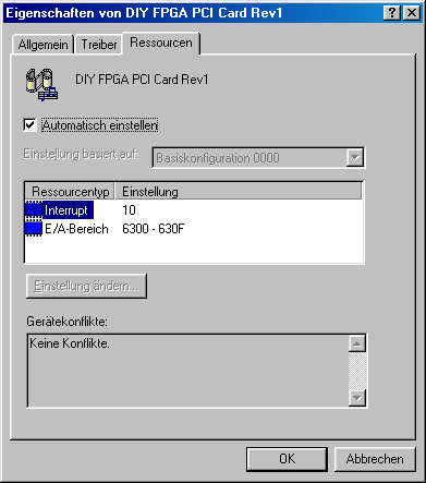
After the basic functions worked correctly, I wanted to test reading and writing to the IO-space to let an LED blink. All IBM-compatible PCs have functions to read/write the IO-space. So I used inline-assembly to write to the desired IO-space. The assigned IO-space can be found in the device-manager of Windows. My card requested 16 bytes of IO-space and the BIOS assigned the IO-address 0x6300 for my card. To write a DWORD to the desired address, I used Borland Delphi 7 to create a Windows-application and I used inline-assembly to write 32-bit to the IO-port:
procedure WriteIOAddress(ioaddress: DWORD; value: DWORD);
begin
  asm
    push EAX; // store EAX-register

    mov EAX, ioaddress; // load address to EAX
    mov DX, AX; // load lower 16-bit to DX

    mov EAX, value; // load value to EAX
    out DX, EAX; // write 32-bit value ("out" uses DX for the address and EAX for the value)

    pop EAX; // restore EAX-register
  end; {asm}
end;
Incredibly this code worked immediatly and the LED turned on, when the corresponding bit was set to high. So I implemented the reading of the IO-space as well:
function ReadIOAddress(ioaddress: DWORD): DWORD;
begin
  asm
    push EAX; // store EAX-register

    mov EAX, ioaddress; // load address to EAX
    mov DX, AX; // load lower 16-bit to DX

    in EAX, DX; // read value to 32-bit EAX
    mov @Result, EAX; // output the value of EAX to function-result

    pop EAX; // restore EAX-register
  end; {asm}
end;
Now I was able to write DWORD-values to my PCI card and read values back as well. Time for more high-level-stuff...
Driver for Windows9x
As the devicemanager of Windows98 showed an ugly yellow question-mark on my PCI card, this was the next thing on my ToDo-list. As Win9x has no driver-signature we can write our driver-files with notepad. So I started a new inf-file. Win9x only wants very few information from us, to put the device in the desired category: a general information about the driver, the VID/PID and some strings:
[version]
Signature="$CHICAGO$"
Class=MEDIA
Provider=%NDNG%
LayoutFile=layout.inf
DriverVer=04/06/2025,1.0.1000.00001

[Manufacturer]
%VENDOR%=Vendor

[Vendor]
%FPGA01.DeviceDesc%=dev.install,PCI\VEN_1172&DEV_2524

[ClassInstall]
AddReg=dev.class.install

[dev.class.install]
HKR,,,0,%ClassString%
HKR,,Icon,0,"-1"

[dev.install]

[SourceDisksName]
1=%DiscDesc%,,

[SourceDisksFiles]

[strings]
NDNG="Noeding"
VENDOR="Noeding"
FPGA01.DeviceDesc="DIY FPGA PCI Card Rev1"
DiscDesc="DIY FPGA PCI Card Driver Disc"
ClassString="Audio-, Video- und Game-Controller"
That's all we need to get Windows to showup the device under Audio-, Video- and Gamecontrollers:
Software
I was curious what I need to play audio-samples using this card. So I programmed a small Windows-application, that reads individual audio-samples from a standard 16-bit Wave-file. The first idea was reading the samples and send them every 22.67 microseconds to the card. As PCI uses a 33MHz clock, this should be possible. But the windows-timer has a minimal resolution of only 1 millisecond - way too long for my simple soundcard. Luckily the Win32-API offers a high-performance counter, that can be used to create much shorter delays:
procedure PerformanceDelay(delay: byte);
var
  hrRes, hrT1, hrT2, dif: Int64;
begin
  if QueryPerformanceFrequency(hrRes) then
  begin
    QueryPerformanceCounter(hrT1);
    repeat
      QueryPerformanceCounter(hrT2);
      dif := (hrT2 - hrT1) * 10000000 div hrRes;
    until dif > delay;
  end;
end;
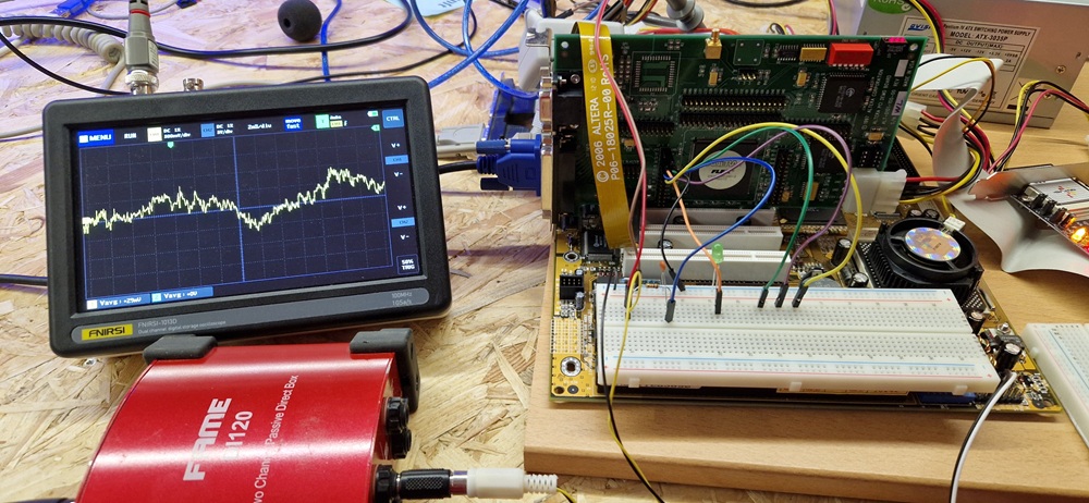
On my Pentium 233MHz I had to call this function with a delay of 75 to send the individual samples with the desired interval. And. It. Worked! I connected a simple Sigma-Delta-Converter to the first 16 bits of the DWORD on IO-Address 0x6300 and using a simple RC-low-pass-filter I received somewhat stuttering and distorted audio.
As my development-card has two 32k x 18-bit SRAM-ICs, my next idea was to create a FIFO ringbuffer using these two ICs to buffer single audio-samples for a better audio-quality. As my FPGA has too few logic-elements for a working FIFO using only block-RAM this was the only option. I will not describe the code for the FIFO-buffer in detail here. The idea is, that on writing samples to the SRAM a variable is increased to show the head of the buffer, while another variable is increased while reading the samples as the tail of the buffer. The distance between head and tail indicates the fill-level of the buffer. As storing 16-bit samples to the 32k SRAM results in a 725ms buffer I decided to use one SRAM-IC for the left audio-channel and the other SRAM-IC for the right channel to keep things easy for the start. Lateron this could be optimized to store both samples in a single SRAM. In Quartus, this looks like this:
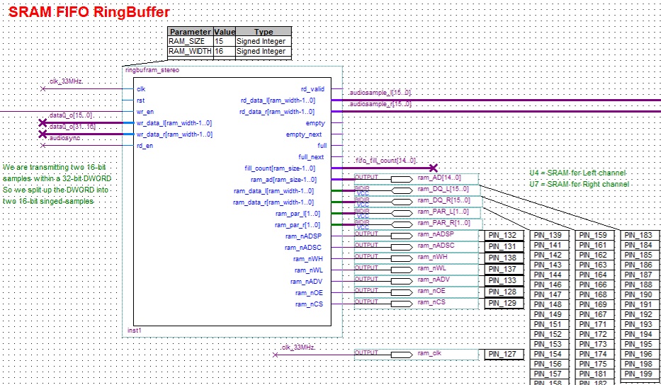
Now that I could store up to 32000 samples to the SRAM-buffer, I changed my windows-application to read chunks of audio-data. I used an individual audio-thread to keep the user-interface responsive. Within this thread, I check the fill-level of the SRAM-FIFO every millisecond and transmit a chunk of new audio-samples if the level is below half of the user-defined buffer-size. The individual samples are then put into the SRAM-buffer and the head-counter is increased. Every 22.66(!) microseconds the FPGA reads an audio-sample from this buffer and transmits it to the Sigma-Delta-Modulator to output the data on an FPGA-pin to the real-word. I've chosen 22.66 microseconds, because my FPGA is clocked by the 33MHz of the PCI bus and 748 is the closest integer-divider I could use to get close to the 44.1kHz (44.117kHz).
I couldn't believe it, but on the first try one of both audio-channels worked fine and played stutterfree music. The other channel produced just loud noise. Here I have to check if the SRAM-IC is working fine or if I mixed up some data-lines.
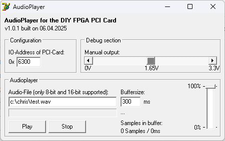
In the Windows-application I added some functions to set the audio-volume (simple multiplication of the signed 16-bit values with the value of the volume-slider) and a display of the current state of the FIFO-buffer:
Outlook
This was part 2 of this series and my DIY PCI Card already can do more than I've expected. Next things on the ToDo-list are fixing the second SRAM-buffer and implementing and testing the memory-space. But as I'm already able to transmit large amount of uncompressed audio to the card, lot of different functions can be implemented: DMX512 outputs for my Retro-Computer to control lights, create additional UART-ports, create measurement-devices and more. As the card has an VGA-connector, this might be the next thing I'd like to have a look. Stay tuned for part 3...
Comments