A kind of diary of reverse engineering the Behringer X32 to finally process audio with my own audio algorithms within the original audio DSPs...
My original plan was to publish a new blog-entry every week. But my current projects got much bigger than I've initially planned. So for the sake of the projects, I will only write new blog-entries,when I have something new and interesting to report.
In my last blog-entry a couple of weeks ago I showed how I started Linux on the Behringer X32 using the bootloader of the NXP i.MX25 microcontroller. The X32 Fullsize has an accessible reset-switch and a boot-mode-switch to enter the bootloader of the i.MX25 - I guess for the case that someone messes up with a firmware update:

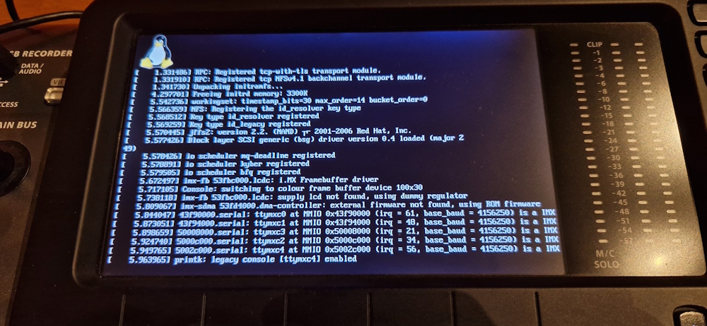
After uploading a binary-blob containing U-Boot (a bootloader compiled for the i.MX25), Linux (compiled for the ARMv5 as well), a Linux-device-tree and an initial file-system (InitramFS), Linux started in under 6 seconds on the audio mixing console:
 So far, so good. I had my first self-compiled Linux-system up and running, but what is the benefit of having Linux on this machine? Well, Linux is totally versatile and brings lot of different drivers for special functions and offers easy to use interfaces to use these functions in C-programs.
Understanding the i.MX25 and having fun with software
It took me a couple of days, but I managed to initialize all important parts of the microcontroller using the device-tree of linux:
- USB-stack
- Ethernet-interface and TCP/IP-stack
- SPI-interface
- UART-interface
- GPIO-pins
- I2C-interface and the realtime-clock of the X32
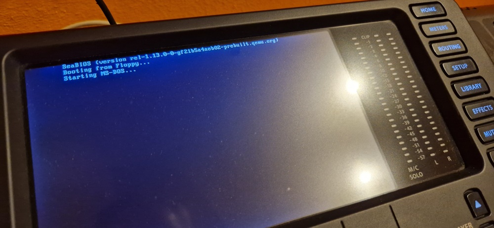
Now that my hardware of the main-controller was under control I wanted to get familiar with the ARMv5-controller and Linux itself. Since I seem to love setting myself ambitious goals and then agonizing over how to achieve them, my idea was: why not run MS-DOS on this system? Yes, stupid idea, I know. MS-DOS has been written for an x86 in x86-assembler, so there is no way to cross-compile this operating system.
The only way is to emulate an x86-system using QEMU. As I said - stupid idea. So I checked out QEMU from the sources, and cross-compiled it for the i.MX25. If you are interested in some details, I packed everything together into a GitHub-repository: X86-on-X32. But it worked quite well and DOS is quite usable and responsive:
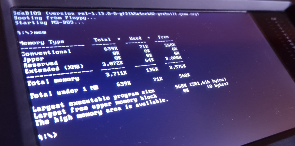
The i.MX25 has some external 64MiB-RAM so QEMU can offer some MiB for the DOS-system which leads to 3.5MiB free RAM after booting DOS:
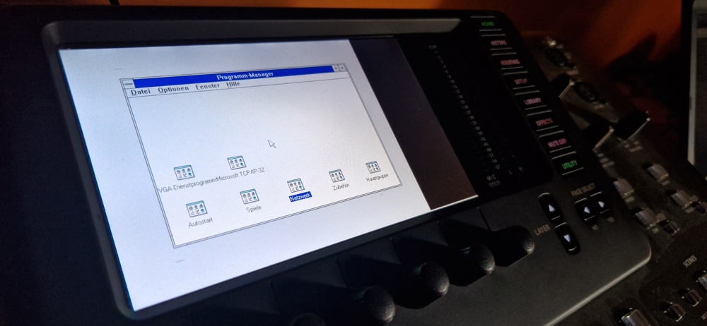
So my next thought was: wow, DOS is running. Why not go one step further and test the limits with Windows 3.11 which was my first graphical user-interface in 1994 besides IBMs OS/2. So I prepared an QEMU image with DOS 6.22 and Windows 3.11 on my computer and configured QEMU to load from this disk-image. Lets ignore the pain I had to find a working combination of QEMU-settings and enjoy the following two pictures:
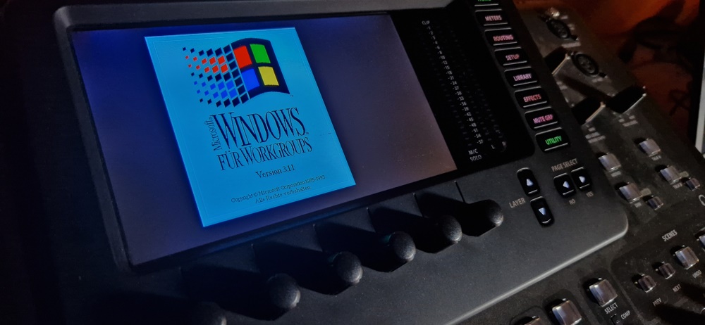
The program manager loads, but it takes foreeeeevvaaaaa. After around 5 minutes the program manager is visible. Keep in mind that this experiment was to check the limits of Linux on the X32 - and I think I crossed a line now :-)
Investigating the interconnection between individual components
Lets go back to something useful. As Linux is working very well and responsive with a recent kernel, I started investigating the connections between individual components. We have to separate the digital audio-connections and the control-lines. For general digital communication the i.MX25 offers two different type of serial interface: SPI and UART. The FPGA is one central component that allows rerouting and distributing the UART-connections:
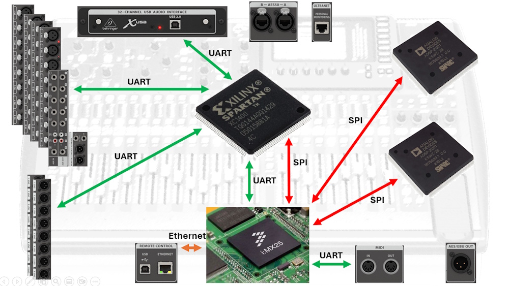
As you can see, the two Analog Devices SHARC DSPs and the Xilinx Spartan 3A FPGA are connected to the SPI-interfaces. Looking into the datasheets (each around 600 - 800 pages) I learned that both devices can be configured using plain SPI. So first I had to get in touch with the FPGA. No problem, I thought. I've already worked with Intel Cyclone 10... but it took me much more effort than expected, to get the Xilinx software up and running...
Creating a bitstream for the Xilinx Spartan 3A
The used Xilinx Spartan 3A XC3S1400A is a quite old device and the last software that supports developing FPGA logic for it is Xilinx ISE 14.7 from the year 2013. As Xilinx has been bought by AMD in 2022 some of the old servers get shut down - an important detail as the installer seems to get in touch with one or more of them - resulting in a fatal endless loop. Thankfully AMD offers a virtual machine with an preinstalled version, but I wanted to use it on my main-machine. In summary I had to kill two background-softwares at a specific part of the installer, add environmental-parameters for Windows to prevent ISE14.7 to check for some VisualC++ components on start and I had to fix a couple of DLLs as ISE14.7 makes use of a software called SmartHeap, that Windows 11 is blocking due to security issues.
Another days later I was able to synthesize my own logic for the FPGA. First I've implemented a basic UART-interface to establish a communication between the i.MX25 and the FPGA itself. Then I added my already prepared TDM8 sender and receiver for the audio as the individual XLR boards for input and output as well as the DSPs and the expansion card are using this type of connection.
For uploading the created programming file (the FPGA-bitstream) I programmed a small linux-program that opened and configured the SPI-interface, asserted the FPGA-PROG_B-pin to initialize the configuration and transmit all bits of the configuration-file. This worked quite flawlessly and I was able to configure the X32-FPGA with my own logic.
Once ISE14.7 was working the implementation of the individual parts was fun again. Next to the TDM8 and UART I implemented some SPI-interfaces to configure the CS2000 PLL-IC as well as the Cirrus Logic Audio-AD/DA-converter that is used for the AUX-inputs and outputs, the talkback-microphones as well as the control-room outputs and headphones.

A tricky part was the 1:1 routing-function that the original X32 has since a later version. For this I've implemented a dual-port block-RAM. All 112 input signals with 24-bit are written within one single audio-cycle (20.83µs at 48kHz). After writing these 112 samples the block-RAM is used to feed all 112 output-signals with the desired input-signals. As the logic-block got quite large, my first attempt of clocking the block-RAM with my designated 100MHz failed. But using much slower 16MHz was the solution: each 24-bit sample now takes 62.5 nanoseconds to read or write, resulting in 7µs for writing to the block-RAM and another 7µs for reading the audio-data to the outputs. That's totally fine and fits well between the 20.83µs of the audio-samples.
Accessing the faderboards and the AD/DA-converter-cards
Now that the FPGA can act as the glue between the individual digital systems, it was time to get in touch with the individual boards like the XLR-inputs and outputs as well as the faderboards. The X32 uses dedicated boards with each 8 channels for input and output and the AUX in/out is located on the main-PCB. The fader-boards have a similar structure and consist of each 8 faders, 8 LCDs and several buttons.
While tracking the connections between the main-PCB and the individual fader-boards I realized, that all boards are daisy-chained using a single UART-connection which makes the communication quite easy. The UART of the AD and DA boards are connected to the FPGA, and is fed to the i.MX25. In total the i.MX25 has 5 UARTs:
- UART = Debug UART, only connected on the main-PCB
- UART = Surface-Boards with Faders, LCDs and Buttons with 115.2kBaud
- UART = AD/DA-Boards and Expansion Card with 38.4kBaud
- UART = FPGA with 115.2 kBaud
- UART = MIDI input and output (used for Linux terminal at the moment)
To understand the communication-protocol of the faderboards and the ADDA-boards, I hooked up an oscilloscope to the individual connections and had a look on them:
It turns out, that the communication is quite simple using a dedicated header and tail together with a kind of checksum at the end:

So the protocol starts with a 0xFE and looks like this:
0xFE, 0x8i, class, index, data[], 0xFE, chksum
- 0xFE = Startbyte
- i = Board-ID
- class = class-ID (e.g. 'L' for LED)
- index = used to identify individual parameters
- data[] = payload
- 0xFE = endbyte
- chksum = ...
Yes, the chksum... I pondered around for this for hours, wrote down tens of papers with recorded commands, and came up with this idea:
Checksum = 0xFD - (sum of all preceding bytes)
As soon as I got negative values, I filled with 0x80 until the value becomes positive again, and if I was above 0x80, I reduce with 0x80. So far, this seemed to work for short messages. But for longer messages this calculation no longer seemed to work and I got incorrect checksums.
As this took me more than a day pondering about this, I took a joker. Due to my Youtube videos about the X32 I got in touch with a couple of nice guys. One of them has put his face as an icon in the X32 original software, when you scroll down the icon-list... yes, try it out :). I contacted him and he gave me the important and missing hint:
chksum = ( 0xFE - i - class - index - sumof(data[]) - sizeof(data[]) ) and 0x7F
I was close with my idea of subtracting the sum of the bytes, but I was missing the subtraction of the size of the data-array without the boardID, class and index. After receiving the missing hint, the scrippt stip LCDs lit up successfully:
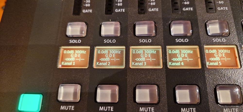
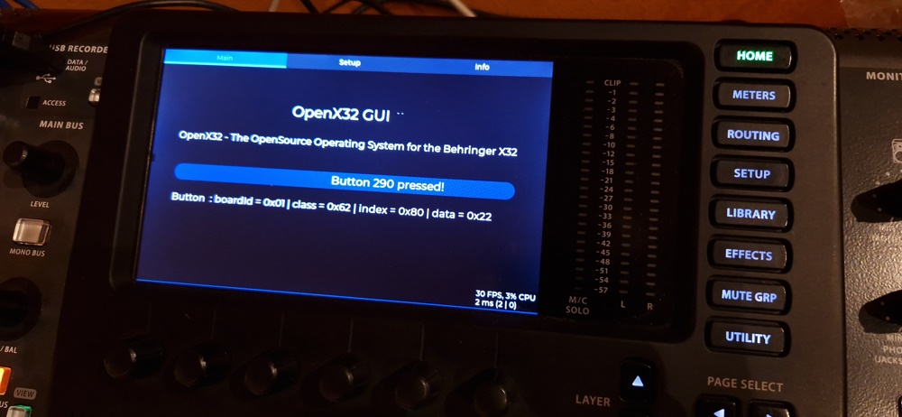
Now that the LCDs were working, it was easy to read out the buttons and control the LEDs. To simplify the task I added a text-field to the LVGL GUI that shows me the individual messages for each button. With this I created a full list of all buttons and associated LEDs and finally got full access to the whole hardware-surface of the X32:
One step further: the Analog Devices SHARC DSPs
There were still two mysterious ICs on the main-PCB, the two Analog Devices SHARC 21371 DSPs:
I never got in touch with DSPs before, but was aware what they are able to do. These two ADSP-21371 ICs are able to process nearly 1.6 GFLOPS, which means up to 1.6 billion Floating-point operations per second - each IC! While processing 40 channel audio with 48kHz (20.83µs) this means we have 833 floating-point operations per sample available. That should be enough for 92-band Biquad-filters (EQ) with each 9 FLOP or other calculations like volume-control as each multiplication, sum or subtraction is counted as a single FLOP.

But first I had to get in touch with another toolchain: how to develop DSP-programs? Using Google it told me lot about DSPs in general, but as the ADSP-2137x is a around 13 years old, its quite challenging to find the most recent tools as the current tools do not support the SHARC DSPs. I've found lot about the Analog Devices SigmaStudio and how someone could implement equalizers, dynamics and more using a graphical environment. But after installing the SHARC-extensions for SigmaStudio I was not able to configure pins and other parameters for my specific chip. It turned out, that this was the wrong toolchain.
After more investigations I realized, that VisualDSP++ is one of the tools for the ADSP-21371. But this tool had its best time in the era of WindowsXP... The current version of its successor, Analog Devices CrossCore Embedded Studio (CCES), is not supporting the SHARC in the recent version 3.x, but version 2.x is looking promising... until you are looking at the price: 1.300US$ - quite a lot for just playing around with it. But luckily Analog Devices is granting a 90 day trial of this software - and I requested some support for my OpenSource project and they granted me an additional 90 day licenses, so I have half a year for testing and developing now, yeah!
So I started CCES, created a new project and... well, yes, and now? I expected some nice GUI to program my DSP. But all I found was a text-editor with C-code and options to compile my code. Obviously this software expect me to program the DSP in plain C. No problem, download some examples to initialize all components and how I can receive TDM8 audio signals from the internet and use this as a reference. I found plenty of code examples for the ADAU1701 DSP and other smaller DSPs, but close to nothing for the 2137x or 2136x series. After some time I learned, that the Analog Devices forum was quite helpful and offered some code-snippets.
It didn't help, I had to study the hardware datasheets. After download two 8 MiB files I realized, that there two main-files, the processor hardware reference and the processor programming reference. The first document had 898 pages, the latter 694 pages... man, I started crawling through the documents and made lots of notes on lot of papers and piece by piece I started a C-project for the DSP. As I published the code on GitHub in the OpenX32 repository, I will not go into details here. But the general idea is as following:
- automatically read the TDM8 data streams from the FPGA using one of the 8 very powerful serial-ports (SPORT)
- use Direct memory access (DMA) to write a predefined amount of samples in the internal RAM
- loop through all received samples, process the samples
- write the processed data to another RAM-position
- output this RAM-part via DMA through another SPORT-channel as TDM8 back to the FPGA
Luckily the DSPs have a single LED for basic debugging. So even I configured the serial ports according to the manual I programmed a counter in the main-loop to let the LED blink. After no compilation errors occured I wanted to test my new code. But how? Back to the manual... But there were no detailed information about how to upload the code without a JTAG-connector...
After more investigation I've found the "Engineer-to-Engineer-Note" EE-177 about "SHARC SPI Slave-Booting" and EE-374 about "Boot Kernel Customization and Firmware Upgradeability on SHARC Processors" as well as the "ADSP-21489 SPI Slave Booting procedure". All three documents helped me to figure out how to configure CCES to output the right output-file format as 8-bit loader-file with default DSP-Kernel. I already had a linux-program written for the FPGA to upload binary-files via the SPI-interface, so I adapted this program for the need of the DSP. Mainly this was the configuration of sending the LeastSignificantBit (LSB) first.
But guess what, I lost one full day learning that the Linux driver is not supporting this mode on the i.MX25. So I had to write my own bit-reorder-function and the LED on the DSP lit up. I remember this moment very clearly: I was totally frustrated that !nothing! worked for more than one day. I got totally stuck with the DSP - I had no clue where the problem was: in my CCES-project, one of the multiple DSP-options, in the pin-configuration, in the configuration of the loader-file, in the DSP-kernel, in my Linux-SPI-uploader-code, in the reset-signal of the DSPs, somewhere. Then I changed the order of the bits manually, just because I was totally lost, I started the upload-program and seconds later I looked in this small yellow LED. Just stared at it. Totally calm. And then you have to remember StarTrek II - the well known "Khaaaan"-Scene.... what a relieve. But I'm getting off-topic.
Reading more of the 1,600 pages main-documentation I was finally able to configure the SPORT interface to receive audio-samples with a buffer-size of 16 samples, leading to a latency of 333µs. First I implemented a simple passthrough but within a couple of days I managed to implement a noisegate, a parametric EQ and a compressor - per channel. As I'm still not used to the SIMD (Single Instruction Multiple Data) option of the SHARC DSP I'm limited to process 8 channels with 16 samples at the moment, but I'm totally fine with this: I managed to program a SHARC DSP in plain C within a closed system without Debugger or any other support.
The first DSP receives in total 5 TDM8 streams from the FPGA (32 regular audio inputs and 8 AUX-inputs) and sends 5 TMD8 streams (16 output channels, 16 P16/UltraNet channels and 8 AUX-channels). The second DSP receives audio from the first DSP but also receives a stereo audio from the i.MX25 and creates the stereo AES/EBU data for the X32Fullsize. Up to know I tested the upload to both DSPs, but focussed on the main DSP first.
The final system
On end of August 2025 I teamed up with another Guy who had interest on working on this project. He pushed the GUI and contributed lot of lines of code and implemented a very nice structure to support the hardware-surface and the GUI. In general the new main-control-software could be developed to reach an early alpha-stage. The software can be started right from the linux-shell with some parameters to load the FPGA- and DSP-configuration:
./x32ctrl -fpga fpga.bit -dsp1 dsp1.ldr -dsp2 dsp2.ldr
The software then loads some nice ASCII-art, configures the FPGA and afterwards one or both SHARC DSPs with the desired configuration-files:
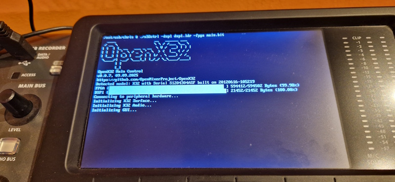
When all components are initialized correctly, the LVGL-based GUI is loaded:

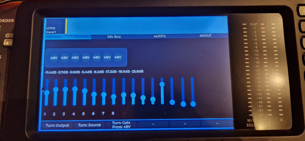
The very first steps are done to create nice and clean user-interface:
Outlook
Within 8 weeks I managed to reverse engineer a couple of different protocols, interconnections between totally different integrated circuits (microcontrollers, analog-digital-converters, FPGA, DSPs, etc.) and create an OpenSource eco-system of a nice hardware. The sound of the DIY-system does not sound different to the original system, so I'm quite confident, that the first steps towards an alternative operating system for this audio-mixing console are in the right direction.
But my plans are not to copy the Behringer X32 operating system, why should I - it's easy to use, doing its job great and it's not annoying the user with stupid things. My goal is to enhance the system in special parts. I'm thinking about a realtime stereo-decompositing algorithm to upmix stereo sound to 5.1 or 7.1 for my home cinema, or implement some other new algorithms in the DSP. You might ask: where is the point? There are devices that you can buy. Sure, but learning new things and getting in touch with new technologies is my drive. I'm not aiming for a device that is developed to 100%, but the first 80% would be fine :) A stereo-decompositing algorithm in the frequency domain takes around 120 and 200 MFLOPS - remember the ADSP is able to process 1.6 GFLOPS.
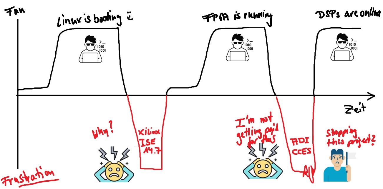
At the very end I'd like to end this blog with my Fun/Frustration-over-Time-Curve of the past 8 weeks. On the two very hard dips I was about to give up. Mainly because I could not get in touch with the necessary toolchains in both cases: the FPGA with ISE14.7 and the DSP with CCES 2.12. But I'm really glad that I did not surrender and I'm able to share my results with you. See you next time!
Comments